
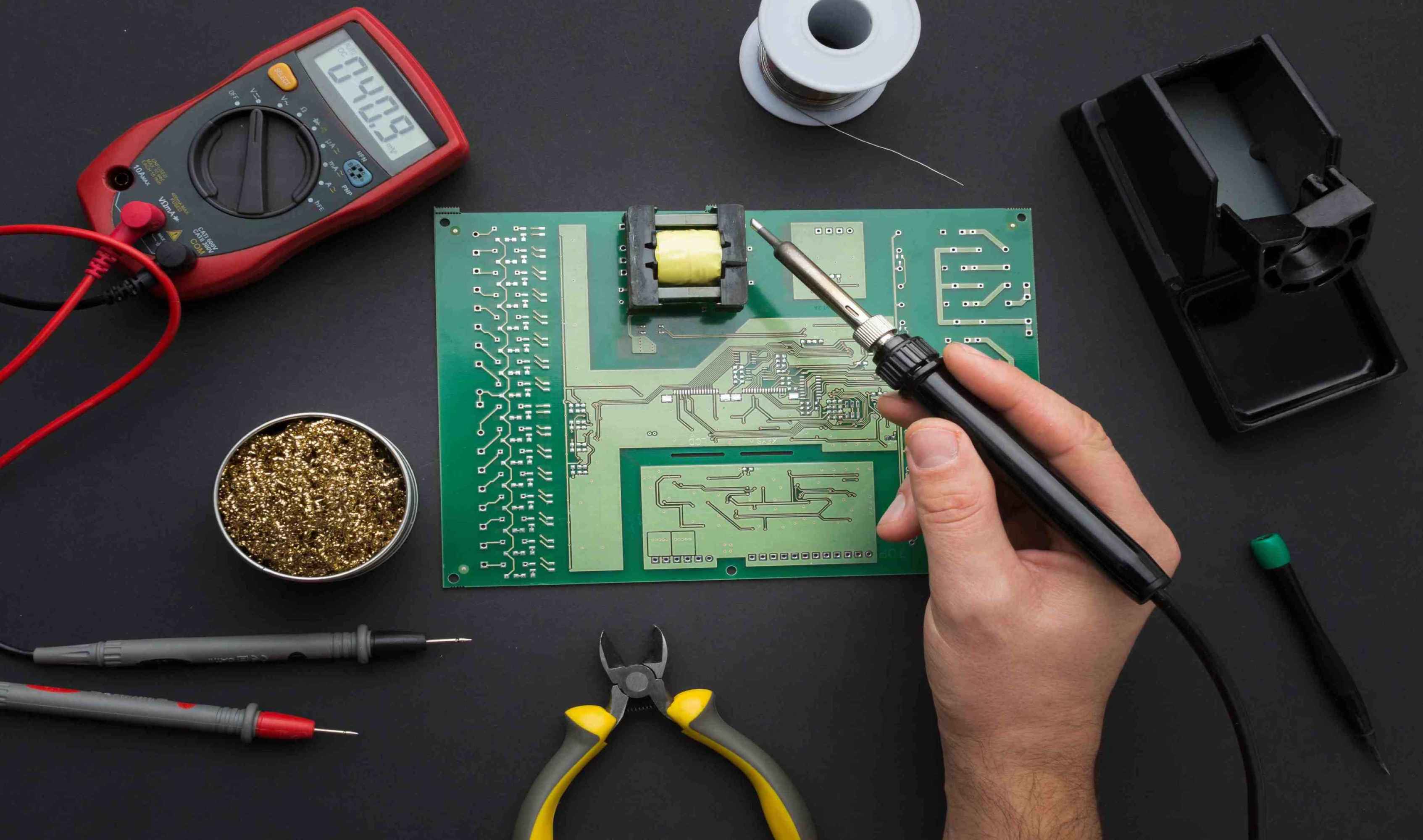
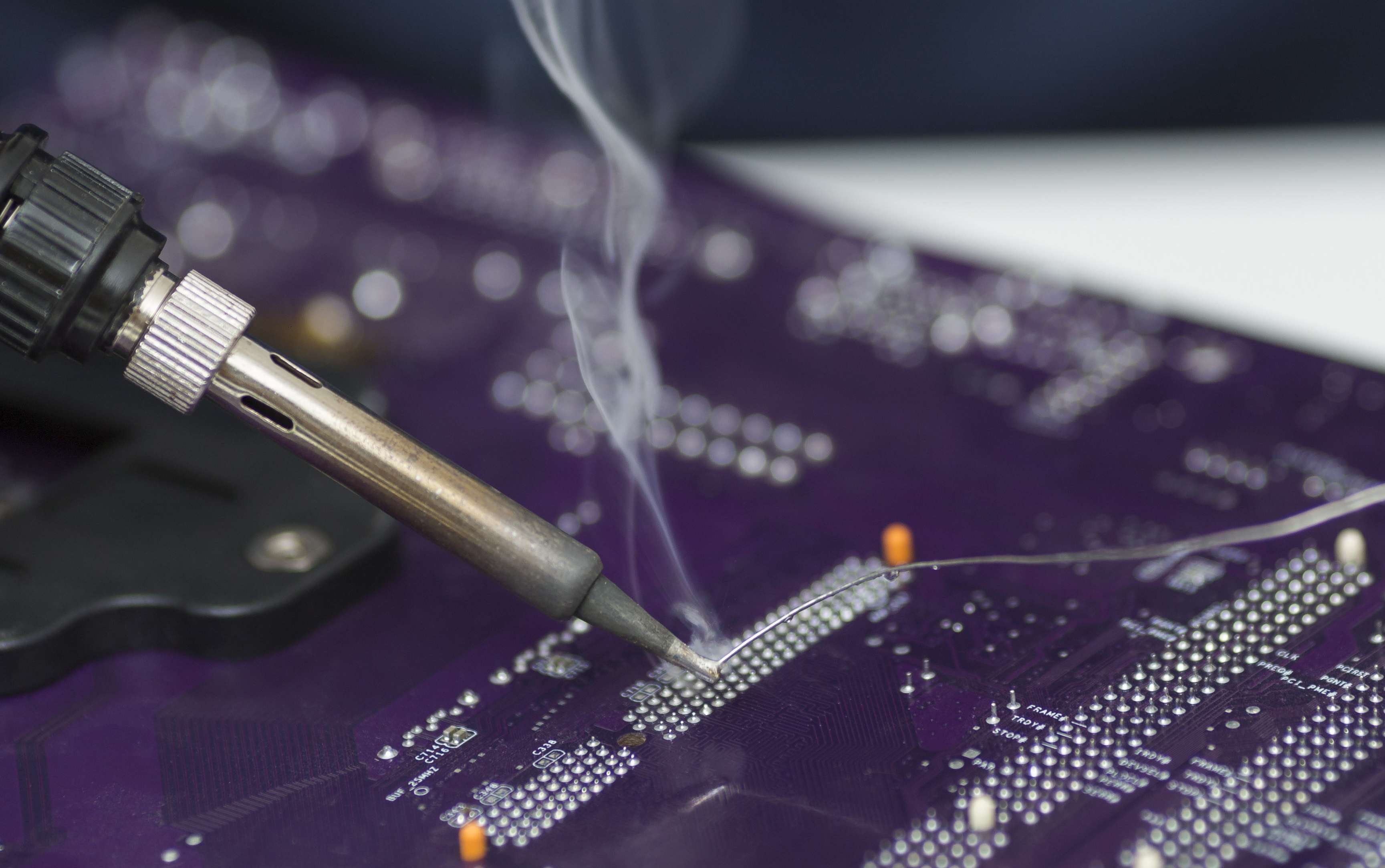
Printed circuit board design and fabrication
Precision PCB Layout Services: Engineering Your Vision into Reality
Precision PCB Layout Services: Engineering Your Vision into Reality
ur focus on quality and speed minimizes risks and accelerates your product’s journey to market. Embien is your trusted partner for PCB layout design because of the following reasons. O
We consider thermal, mechanical, and manufacturing aspects from the start.
More than two decades of combined experience in high-complexity designs.
Designs optimized for manufacturability anywhere in the world.
Proactive validation of Signal Integrity, Power Integrity, and Thermal performance.
Expertise in designing for high-volume production without sacrificing quality.
We work as an extension of your team to achieve shared success.
High-Speed Digital & Analog Mastering impedance control, differential pairs, and timing constraints for interfaces like DDR4/5, PCIe, Ethernet, and SerDes.
High-Density Interconnect (HDI) Expertise in micro-vias, blind/buried vias, and advanced stack-ups for ultra-compact and complex designs.
RF & Microwave Meticulous layout for antennas, filters, and high-frequency circuits, ensuring optimal performance and minimal interference.
Mixed-Signal Design Isolating sensitive analog circuits from noisy digital sections to guarantee signal purity and measurement accuracy.
Power Electronics Designing for high-current and high-voltage applications with a focus on thermal management, creepage, and clearance standards.
Flex & Rigid-Flex PCBs Creating innovative solutions for wearable devices, robotics, and products with challenging form factors.


We consistently push the boundaries of what's possible, navigating complexities such as high-speed signal integrity, dense component placement, power delivery networks, and stringent environmental requirements. Our expertise allows us to engineer robust and reliable solutions for the most demanding applications.
Here are some examples of the complex PCB designs we have successfully undertaken:
We designed a highly dense SoM featuring a complex MPSoC, multiple DDR4 memory chips, and high-speed peripherals. The design required intricate routing with blind and buried vias and precise impedance control across all 24 layers.
A mechanically constrained PCB for a ruggedized eCockpit system. The layout had to accommodate multiple connectors on a single edge while meeting strict thermal and EMI/EMC standards for the automotive industry and ensuring ingress protection.
We engineered an ultra-small form factor design for a next-generation hearing aid, utilizing flexible PCB technology to fit complex circuitry into an ergonomic, non-linear shape.
A stacked PCB design for a telematics unit featuring Cellular, Wi-Fi, Bluetooth, GPS, and LoRa radios. The key challenge was meticulous RF layout and shielding to prevent inter-radio interference.


At Embien, simulation is a cornerstone of our PCB layout process, ensuring flawless performance before production begins. Early validation helps us eliminate issues, reduce costs, and deliver PCBs that thrive in real-world conditions. Our toolkit includes:

Signal and power integrity analysis for robust designs.

Electromagnetic simulation for high-speed performance.

Circuit simulation for analog and mixed-signal validation

Heat management for high-power applications using Flotherm & Icepak.
Our proficiency across these platforms ensures your PCB meets performance, reliability, and budget goals, from two-layer prototypes to 24-layer masterpieces. Embien leverages industry-leading Electronic Design Automation (EDA) tools to craft exceptional PCB layouts:

Perfect for rapid prototyping and intricate multi-layer boards.

Advanced routing for high-speed, high-density designs.

Open-source flexibility for cost-effective, scalable projects.

Streamlined design for small to medium complexity boards.

End-to-end embedded hardware design including schematic development, PCB layout, prototyping, and manufacturing support.
Explore Hardware Development

Understanding black box and white box testing techniques for validating embedded hardware and software.
Learn embedded testing methods

Triple-display automotive ADK integrating Android, FreeRTOS, and multi-display cockpit architecture.
See multi-display cockpit solution

Architecture and control strategies of motor control units driving electric vehicle motors.
Understand EV motor control

Design considerations and enclosure strategies to achieve reliable IP-rated protection in electronics.
Design IP-rated electronics

Semiconductor advancements shaping embedded system design for performance and efficiency.
Explore semiconductor trends
Reach out to our engineering team today. We're ready to tackle your most demanding layout challenges.