
In the fast-evolving world of semiconductor design, AI-aware EDA tools are emerging as gamechangers, streamlining workflows and slashing time-to-market. With chip complexity soaring due to demands for AI accelerators, edge computing, and advanced SoCs, traditional electronic design automation (EDA) methods are struggling to keep pace. AI-driven chip design tools, powered by machine learning in EDA, offer predictive insights, automation, and optimization that reduce development cycles by up to 20-30%. This article explores the latest trends in AI-enabled EDA tools, their features, future roadmaps, and how they accelerate semiconductor innovation.
AI-aware EDA tools integrate machine learning and generative AI into the semiconductor design flow, enabling smarter decision-making across stages like RTL synthesis, verification, and physical implementation. Unlike conventional tools, these AI-powered solutions learn from vast datasets to predict outcomes, automate repetitive tasks, and optimize power, performance, and area (PPA). For instance, reinforcement learning algorithms analyze thousands of design parameters to refine floorplans and routing, cutting re-spins and costs.
By 2026, the global market for 3nm semiconductor EDA AI tools is projected to reach USD 774.4 million, growing at a CAGR of 8.1%, driven by the need to manage extreme design complexity at advanced nodes.
This shift toward AI-native EDA represents a pivotal evolution, where AI is at the core of workflows, handling multimodal data like netlists and layouts.
The EDA landscape spans front-end design (RTL and verification), back-end (synthesis, place-and-route), and manufacturing. Leading vendors like Synopsys, Cadence, and Siemens EDA have embedded AI across this spectrum, with startups like Alpha Design AI and Rapidus adding innovative twists.
In front-end design,
For synthesis and physical design,
In test and manufacturing,
Startups like Alpha Design AI's ChipAgents aim for 10X productivity in RTL verification using AI agents.
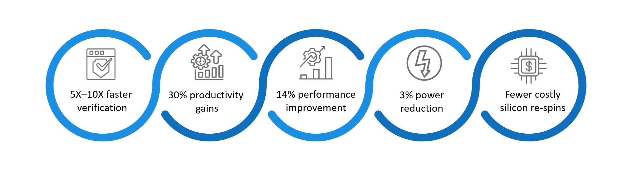
Today's AI-aware EDA tools boast features like generative AI for code generation, agentic workflows for autonomous task handling, and predictive analytics for yield optimization. Synopsys.ai includes GenAI for 24/7 expertise and Agentic AI for workflow automation, yielding 30% productivity gains.
These features connect disparate tools into unified ecosystems, ensuring seamless data flow and reducing manual interventions.
By 2026-2027, AI EDA tools will advance to fully agentic and AI-native systems. Synopsys plans expansions in autonomous 3D design optimization and deeper NVIDIA integrations for GPU-accelerated simulations.
AI in semiconductor design delivers profound advantages, primarily accelerating time-to-market. Tools like Synopsys.ai reduce verification times by 5X-10X, freeing engineers for innovation.
To leverage these, adopt hybrid workflows: Start with AI for initial exploration, then refine with human oversight. Integrate tools like VSO.ai early in verification to close coverage gaps faster.
Use GenAI for documentation and test scenarios, cutting cycles from months to days.
For advanced nodes, employ agentic AI to automate regressions, addressing talent shortages.
Early adopters like NVIDIA and Samsung have seen 25% smaller circuits and optimized Exynos designs. Embien's product engineering services integrate AI-Aware EDA Tools into chip bring-up and BSP delivery workflows, while our semiconductor development support practice helps customers apply the latest AI-enabled EDA tools to cut re-spins and accelerate Electronic Design Automation cycles. AI-aware EDA advancements are increasingly complemented by edge computing services and edge AI development for faster on-device intelligence and optimization.
AI-Aware EDA Tools are compressing semiconductor verification timelines from months to days, with AI in semiconductor design now driving PPA optimisation, autonomous regression testing, and generative RTL workflows across leading Electronic Design Automation platforms. The latest AI-enabled EDA tools represent a step-change in productivity, but realising their full value requires experienced semiconductor development support to translate tool outputs into silicon-ready, production-qualified designs.

Learn how Embien's product engineering services integrate AI-aware EDA workflows to accelerate chip bring-up, BSP delivery, and reference design development for silicon vendors and product OEMs.

Embien's semiconductor development support spans pre-silicon RTL validation through post-silicon EVK and driver delivery — helping teams exploit AI-enabled EDA tools to cut re-spins and time-to-market.

A practical demonstration of AI-aware embedded design: Embien applied TinyML-based anomaly detection on a resource-constrained microcontroller to deliver a production-ready water leakage detection system — showing how AI-Aware EDA Tools translate into shipping embedded AI products.